New enhancements in this release:
(Tip: You can use the Table of Content  on the right side, to view the list of all enhancements)
New Comments Tab in the Information Panel |
|---|
Why Improved collaboration through direct communicating with semiconductor design stakeholders in the comments panel |
How - You can now use the Comments tab in the Information Panel to seamlessly communicate and collaborate with semiconductor design stakeholders.
- You can also tag relevant stakeholders to notify them about your comment.
 |
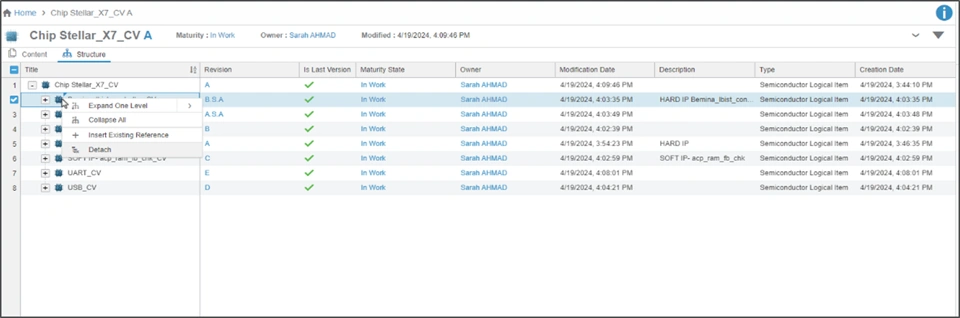
Semiconductor Item Structure Modifications |
|---|
Why Easily view and modify your semiconductor item using the new Structure tab and its context menu options |
How - You can now refer to the new Structure tab to easily view packaging of your Semiconductor Logical Item.
- You can also use the following context menu options to view and modify it as required:
- Expand
- Collapse
- Insert Existing Reference
- Detach
 |
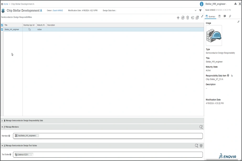
Semiconductor Design Environment Management |
|---|
Why Improved productivity using a single app for managing design environment, team, tool and workspaces |
How - The semiconductor development project managers or administrators can now use the “Semiconductor Design Environment Management” app to perform the following activities:
- Create semiconductor design environment
- Define & manage the design responsibilities while working on common development projects
- Manage semiconductor design data
- Manage the semiconductor design tool suites
- You can use the Copy the Desktop App URL and the sde create command to initiate design environment and area. Further, you can use sws command-line to launch your preconfigured semiconductor design tool to reduce startup time
 |
🎬 To discover more about these enhancements, watch the video below:
If you have any question or comments on this highlight, please share them with us below. 👇
Thanks!

